Getting the transcript
Reading the captions from YouTube. A video nobody has opened here before takes 10 to 30 seconds; this page fills in on its own.
Getting the transcript
Reading the captions from YouTube. A video nobody has opened here before takes 10 to 30 seconds; this page fills in on its own.
Breaking Taps · @BreakingTaps
Words
5,544
Runtime
33:09
Speaking pace
167wpm
Reading time
23min
167 words per minute, between the 160 25th percentile and the 181 median of 349 measured videos. That distribution comes from the 349-video hook study.
Opening (first 30 seconds)
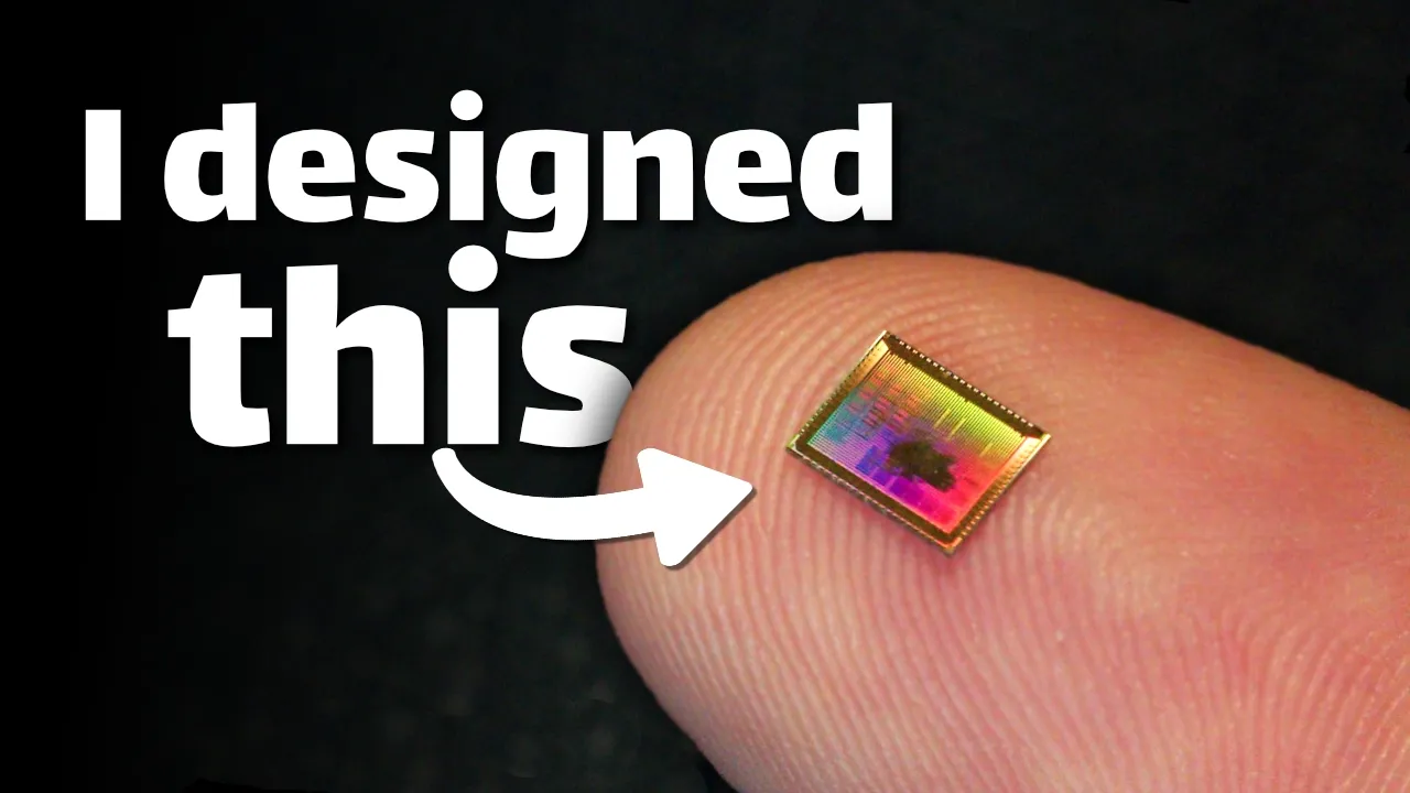
There are millions, probably even billions of chips in the world at this point, but this one, this is special because I designed it. This is Breaking Taps, a custom microprocessor that I designed and sent to a real semiconductor foundry to be manufactured. This was a really tough project, and I want to tell you all about it. It is 3:30 in the morning, but I've been working on this mess. [laughter] It's working. >> The story starts about a year ago at
84 words, the words spoken in the first 30 seconds at 167 words per minute.
Free, no signup. See how the first 30 seconds hold attention, with rewrites.
Sentence shape
| Measure | This transcript |
|---|---|
| Sentences | 387 |
| Average words per sentence | 14.3 |
| Longest sentence | 59 words |
| Questions asked | 9 |
| Sentences containing a number | 21 |
Most used terms
Filler phrases
116 in total: like 37 · uh 25 · basically 14 · kind of 13 · actually 11 · you know 6 · right? 4 · sort of 3 · um 2 · literally 1.
A literal whole-word count of the same phrase list the Prepublish browser extension uses, so a phrase inside another word is not counted and a phrase used in its ordinary sense still is. It is a count and not a judgement.
Run the check on the words above: where attention is likely to drop, with a rewrite for each weak line. The free check shows the scores and the one issue costing the most.
What this transcript is
Every word below is the caption track YouTube publishes for this video, pulled from the video itself and reproduced unchanged. It is not Prepublish's writing, not a summary, and not a re-transcription: it is the video's own published captions. English captions, generated automatically by YouTube, in the video’s original language. Source: the video on YouTube. A channel that would rather this page did not exist can ask for its removal through the contact page, and it is removed.
No Script X-ray for this video: YouTube shows a Most replayed graph only once a video has enough views.
There are millions, probably even billions of chips in the world at this point, but this one, this is special because I designed it. This is Breaking Taps, a custom microprocessor that I designed and sent to a real semiconductor foundry to be manufactured. This was a really tough project, and I want to tell you all about it. It is 3:30 in the morning, but I've been working on this mess. [laughter] It's working. >> The story starts about a year ago at OpenSauce where I met this guy Tim.
Tim had just started a company called Wafer.space whose goal was to offer affordable open-source multi-project wafer services. Open sauce was in June or July of last year. I was in the middle of a big cross-country move at the time and I didn't really think anything else of it until about November. I had sold off my shop. I had driven literally across the country and resettled on the West Coast and I was looking for some projects to work on.
And for whatever reason, I decided that designing and taping out a chip seemed like an easy and fun thing to do. [laughter] There was really only one problem, though. Well, maybe two problems depending on how you look at it. First, I have never done any chip design before. Never even used an FPGA. My electrical engineering skills are pretty trash. I really don't know what I'm doing. So, I'd be starting completely fresh.
So, we can expect there'll be at least a bit of a learning curve to get going on this. And that makes the second problem, well, a little more problematic because I only had 1 month to finish the tape out before the deadline, which is fine. Totally fine, right? We're not panicking. I'm not panicking. You're not panicking. It's going to be fine. Chip design, walk in the park. It's not like it's rocket science or anything.
Just semiconductor. It's just chip design. I'm just designing thinking sand. So, the first order of business is choosing a project to work on. It should be relatively simple because we only have a month to get this thing done, but it should also be interesting and unique. If we're going to go through all the hassle of taping out a custom design, it should be something that you can't just buy off the shelf. So, I went digging through old processor ideas and settled on something called transport triggered architecture or TTA.
Say we want to add two numbers together. In a normal processor, you'd simply execute the add instruction and tell it to add register 1 to register 2 and place the result in register 3. Pretty straightforward. A normal processor is all about telling the hardware what to do, what instructions or operations to execute. In contrast, PTA is all about data movement. You move data into the ports of functional units and operations happen as a side effect of that data moving around.
So, we move register one into the input port of the adder and move register 2 into the trigger port of the adder. This automatically causes the adder to execute the operation, add the two values together, and places the result in its output port. We then move that into register 3 ourselves. The difference here might feel a little academic. They're ultimately doing the same thing, just a different way of kind of encoding the operation, but this actually translates to a simplification on the hardware side of things because the hardware no longer really needs to care about how to schedule and decide where data moves because the compiler chooses all that for us.
So, it's taking some of the complexity and moving it up to the compiler rather than building it into the hardware itself. Okay, [music] so we know what we want to build. How do you actually design a chip? I try to [music] picture clusters of information and they move through the computer. No, it's basically programming uh except with different languages and everything happens everywhere all at once. If you want to learn to design a chip professionally, go learn Verarilog.
It's the main language that's used and there's really no getting around it. The language kind of sucks, but what are you going to do? But if you want to have fun, you can pick any of the more modern HDLs. I chose Spade, which is a Rust inspired language and has some really interesting features. At the surface, Spade looks a lot like a normal programming language. We can define two variables and assign them some values.
But what's unique about hardware design is that these two statements happen concurrently. A and B are evaluated and assigned at the same time. When this is converted into transistors, there'll be a circuit that calculates the addition and another circuit that calculates the multiplication. They receive inputs simultaneously and both execute in parallel. But if we adjust the code so that B depends on A, we've now linked the two circuits together into one logic cone.
So now the adder circuit has to fully resolve before we can multiply. In spade, you'd often put this kind of code inside of a function. This general style of code is called combinational logic, but programmers might know it better as a pure function with no side effects. Inputs enter, some computation happens, and then outputs leave. There's no hidden state that mutates anything. No side effects. This is in contrast to sequential logic where we are allowed to introduce persistent state.
Spade calls these registers, and under the covers, they're translated into a D flip-flop. Flip-flops look something like this and use 20 to 30 transistors to hold a single bit of information. We can use a register to hold a counter. For example, notice how the syntax specifies a clock. Sequential logic advances on each clock cycle. So the register state is tied to that clock's edge. So each time the clock cycles, the counter value is incremented.
Of course, sequential and combinational logic can be combined. If we only want to count from 0 to 9, we could do this. The value of our counter is equal to zero if the current count is nine. Otherwise, the value is incremented. This if statement looks like a conditional execution, but is actually two separate circuits that are evaluated at the same time. One circuit will generate a value equals 9 comparator, and the other circuit calculates the value after it's been incremented.
And these both happen concurrently, which is very different from how normally you'd think about programming. Finally, a multipplexer selects the correct branch and passes that onto the register, throwing away the other branch that's not used. Now, if I'm being honest, I had no idea how any of this worked when I first started. I just knocked out a bunch of code as if I was programming, wrote a bunch of tests, and got something that was working.
But in retrospect, I could have optimized my chip a lot had I known these details. So don't let this hardware stuff get too into your head. You can do a lot of really interesting work without understanding what exactly is going on at the transistor level. But as soon as you start to dig into the details, your hardware will become much much better. As an example, let's try to calculate a dot product. Pretty simple, right?
Translated into spade, we'd get something like this. Knowing about combinational and sequential code, you can see that this is all combinational. Not a single register in this whole function. When we synthesize this into real transistors, this is the result. Inputs are over on this side and outputs are over here. Wires glow based on actual simulation data. So this is a fairly realistic animation of what's going on. As soon as inputs enter the circuit, electrical activity races through the network and appears at the output side.
This works great as long as the activity can reach the end before the next clock cycle. There's a real physical speed to how fast transistors can switch, which means circuits that are deep and complicated run the risk of not finishing in time before the next clock cycle. This is known as a setup timing violation. And one of the ways to fix this is by pipelining the circuit. Pipelining uses registers to hold intermediate state.
Here is the same dot product but split up with a pipeline of three stages. Spade has special syntax for this but basically it adds registers at these two locations to hold the intermediate state. And here is the final circuit. We can see a reset line, a clock line, and two sets of flip-flop registers which correspond to the two stages of our pipeline. When the circuit runs, it takes several clock cycles to reach the output.
But in exchange, only a third of the circuit needs to complete before the next clock cycle compared to the original. The latency of one input is now three clock cycles long. But once the pipeline is full, the throughput is the same. We get one result every clock. Here's an even more dramatic example. This is a 32bit multiply and accumulate function. A and B are multiplied together. And because both values are 32 bits, we need 64 bits to hold the resulting product.
Then we add our product into the running accumulator and return the sum. Super simple, right? Just two lines of code. Unfortunately, the code synthesizes into this monster. Our simple two lines turns into a giant circuit that is many levels deep. You can see how long the activity keeps ticking through the circuit. And since this is all combinational, all of this activity has to finish before the next clock cycle. Real chip designers would know that a MAC operation like this needs to be pipelined.
And unfortunately, I'm not a real chip designer. So, I actually made this mistake in my chip. Here's a rough overview of the functional units that I implemented. And here is a multiply and accumulate block. Look at how much space that takes up. And more importantly than space, this thing caused a bunch of timing problems for me. I really struggled to hit my target clock speed and I didn't know enough at the time to properly debug and troubleshoot it.
But it was because of this unpipelined multiply and accumulate unit. So now that you know how HDL's work, or at least at a high level, we can start to design the microprocessor itself. This is a high-level overview of the BTAP's chip laid out like you'd see it in the TTA literature. This is generally the format that they show things. So you can see in the middle we have these two data buses which connect to all of our various functional units.
For my design, every functional unit is connected to both buses. But this doesn't necessarily have to be true. There are lots of designs out there that will have say four or eight buses and some of the functional units are only attached to some of them but not others. The code is organized just like you'd expect from any normal programming project. There's a main entry point called chip top which does all the setup of the SPI and UART the boot loader stuff like that.
So we won't get into this at the moment but let's go take a look at the ALU. So the ALU or arithmetic logic unit performs all your basic math operations. You can see here is an enum at the top which defines the different instructions it knows how to process. So we've got like add, subtract, and or not, stuff like that. The core of this alou is this pattern match here where we look to see what the trigger is. So it's an alou op, which is this enum.
So we look up the instruction we need to execute. That's on the left side here of this pattern match. So find the instruction we care about. Say we want to perform an addition. Then once we've matched the token, we perform the actual operation which in this case is just adding operand A to operand B and then this is returned. Super simple. Some of them are a little more complicated. So it' be annoying to put inline. So for example, the unsigned saturating addition is sent down here to a function.
But this is just for, you know, making the code look a little nicer. And every other functional unit is basically set up similarly. So, bit manipulations, same idea. We've got our instructions on the left here, and then our actual operations on the right. Editing taps here. So, in reviewing the footage, uh, I started to go pretty deep on the design of the microprocessor and how some of the more speedy details work. And, well, this video was getting really long and we have a lot still to cover about the whole process.
So, I'm going to punt all of the microprocessor design into a new video where we can really dig into like how the architecture works, the things I learned along the way, the bugs I ran into, stuff like that. I know folks will be interested in the specs of the chip. So, it should run 18 to 20 megahertz give or take. Uh there are two 32bit data buses and it can execute two instructions per clock cycle which means it is technically a supercaler processor which is kind of cool.
Program memory is 1,024 slots long and each slot is two instructions. So a program can have a total of 248 instructions. There's a 256word stack, 4 kilobytes of general purpose RAM, uh, and 80 or so different instructions spread across like 20 or 30 functional units. Uh, this includes stuff like branching and comparisons, math operations, bit manipulation, random number generation, stuff like that. Uh, finally, there are 16 general purpose inputs, 16 general purpose outputs, an SPI, which I just recently learned is completely broken, so that's unfortunate.
Uh, a UART, which is kind of broken, but should be salvageable. Uh, and an 8bit parallel bootloading interface to get the program onto the chip. Oh, right. Uh, testing of the chip. So, there's the correct way and the easy way. Uh, you should probably do both of them, but I mostly did the easy way. So, the correct way is to work on your chip and then load parts or all of it onto an FPGA and test out as much as you can in hardware, so to speak.
Uh, it's not a perfect match. There's some things that don't transfer well, like the SRAM blocks on the ASIC are different than the memory blocks on FPGA, but you can test out a lot of the functionality and the timing that way. I didn't do that because of a time crunch and again I've never used an FPGA. So the easy way is to just write a whole bunch of tests. We'll cover this more in the next video, but basically there's a framework that you can use called Coco TB or another program called Verilator.
And these basically simulate the waveforms that would be flowing through your circuit and allows you to make assertions that you know at this point in time or after this certain clock cycle you can assert that these bits are high or low. So, Spade provides kind of an adapter to Coco TV, which is like a Python package, and allows you to assert different things, step the clock through multiple cycles, ensure that different conditions are met, and you can get pretty far with just that sort of testing as long as everything's broken out into, you know, small testable chunks.
At least so far, that seems to have worked pretty well. Again, I do have some bugs that I've discovered uh mostly due to missing tests around certain interfaces and so that's on me. But also, the chip is pretty simple. There's only one clock domain. It's not doing a whole lot of crazy complicated logic. So, you would kind of expect testing to catch most of the bugs. Uh but we'll cover this a lot more in the next video.
But for now, let's look at how we take our spade code [music] and turn it into actual transistors. >> [music] >> Right. So, no one actually handdraws transistors anymore, at least not for digital logic. Analog's a whole different ballgame where you actually do the layout yourself, but that's definitely subject for a different video. Today, just like compilers will generate machine code from your highle programming language, the process of creating all the actual transistors in your circuit and your chip is highly automated.
In the open source world, we use a framework called Liberlane. This is like an orchestration framework that ties together a bunch of individual open- source tools. Wafer.space also provides a Nyx flake which makes the whole process super easy to get going. That being said, it is helpful to know what's going on under the hood and frankly it's just kind of neat. There's a lot of really cool technology and algorithms transforming your digital design into transistors.
So let's briefly look at all the stages of a Libra lane build. The first step is called synthesis and it converts your design into a net list of standard cells. A tool called Yossis extracts all the combinational blocks from your code and converts them into an AND inverter graph. Another tool called ABC tries to optimize the graph by rewriting, balancing, refactoring, removing redundant logical paths, stuff like that.
ABC then maps the optimized graph onto the actual cells defined in your PDK's standard cell library. This is stuff like ands and ores, knots, exors, all the basic building blocks of a chip. At the end of synthesis, we have a full net list of standard cells representing our entire chip. The next major phase is floor planning and global placement and this is executed by a tool called open road. The chip's area is defined and a rough power grid is laid across the whole chip using the top two metal layers.
Then our net list of cells are roughly positioned across the chip. This global placement step is really neat in my opinion. There are a lot of algorithms to do this kind of placement, but Open Road uses an algorithm called replace. The optimizer tries to minimize the wire length of a chip. Basically, how long all the routing wires are between the individual cells. The intuition here is that related components should be placed physically close to each other and the overall circuit should be as compact and dense as possible.
But cramming everything together in one area can be problematic. So replace pretends the layout is sort of like an electrostatic simulation. cells are given positive charge and so areas that become too congested build up a large positive charge which the simulation will naturally spread out. This optimization function, the wire length attracting cells together while the positive charge pushing them away continues iterating until the process settles.
It's a clever and fast way to do a rough layout of all your cells. It's definitely not optimal yet. Later steps will refine the placement, but it's good and it's fast for a first draft. The next step is to estimate the parasitics of our rough layout and then run some static timing analysis of the chip. Open Road will then execute a resizing step where buffers and gate drive strengths are adjusted or inserted. And this is done to help fix timing skew, capacitance issues, large fanout circuits, stuff like that.
We'll be rerunning this resizing optimization step a lot in the future. From there, a detailed placement step is executed which basically legalizes the whole layout. It makes sure that all the various design rules provided by the foundry are actually followed. Most digital logic circuits need a clock. So the next step is clock tree synthesis. This step tries to fan out an even and balanced clock tree to the whole chip.
This is important because an unbalanced tree can lead to skew amongst the different branches which will throw off the relative timing of different parts of the circuit. Another round of resizing and optimization is executed and then we perform global routing. Here we wire up all the cells in the net list. The routing algorithm tries to minimize wire length while balancing congestion across the different metal layers.
We don't have a final set of wires that are DRC legal yet, but kind of a rough draft of where we want all the wires to go. Once global routing is done, we look for excessively long wires and assign diodes to them. This is actually a physical safety check that fabs require. Long wires can act as antennas. And when chips go through various plasma steps during processing, those antennas can collect excess charge and dump it into the gate of a transistor.
Because the gates are so small and fragile, the extra charge can actually burst through them and ruin the device. So this step goes through and adds reverse bias diodes to ground along the length of really long wires. And it basically makes sure that every wire is broken up after a certain distance with a diode to uh dump any excess charge that might build up during processing. We do yet another round of timing based optimizations and then move on to a step called detailed routing.
This is basically like an auto router in PCB software except it's working with millions or even billions of cells and wires. Detailed routing specifies the exact tracks and VAS across all the different layers needed to wire up the cells and make sure that they're legal according to the design rules. At this point, our chip is basically finished and hopefully we have something that we can send off to manufacturing. Open Road will perform a final parasitic extraction of our final layout and analyze the timing of the whole chip.
It will then generate a GDS file which is like the physical layout representation of our chip. We're not quite done yet though. We have two more steps we have to execute. The first is an exhaustive DRC or design rule check. These decks provided by the foundry are enormous and really slow because you have to go through all the different polygons in your GDS and make sure all the rules are followed about like spacing and overlaps and containment boundaries, stuff like that.
This step alone is like half of the runtime of the whole process. In fact, I was under such a time crunch that I ended up renting a really large gaming server just to help process these compilations faster. And on that server, it took about four hours for the whole process to complete. And about two of the hours were the design rules. And this is on an old process node. 180 nm is basically ancient. So the deck itself is relatively manageable.
But cutting edge finfet nodes, I'm told have absolutely enormous and complicated DRC decks, which I imagine take a really long time to run. And then the last step is to run a layout versus schematic extraction or LVS. This basically walks over the final geometric physical layout and extracts the connectivity of all the transistors and you generate a post layout net list. This net list is compared to our original digital design net list from the very beginning and it makes sure that they match.
In effect, it's making sure that electrically we've generated what we digitally designed. And if we get this far, that's it. You're done. You have a GDS file. You can send it off to the fab for manufacturing. This was a super highle overview of the whole process. And in reality, there are a bunch of knobs and parameters which you can adjust and it'll change how the chip is laid out and the timing and performance and all that.
But as a beginner, honestly, you don't really need to care about most of the knobs. You can treat it sort of as a black box. Dump in your code, get a file out the other end. So, you fire your design off to manufacturing. What's next and what should you expect? Well, it varies depending on the shuttle service that you're using, but wafer.space uses Global Foundaries 180 nanometer process, and turnaround time is something like 3 to 4 months.
While you wait, you can hunt for bugs, work on revisions, or build tooling for your chip. For example, TTA is sufficiently unique and kind of weird that I started to build an assembler IDE to make programming it a little easier. I'm also slowly starting to work on a compiler because there are some neat optimizations we can take advantage of in TTA architectures. But after a few months, the bear dyes arrived and I could take my first look.
And I don't know, it's really hard to describe the feeling of holding a piece of silicon in your hand that you've designed. It truly was amazing. It's also just really cool to look at your chip under a microscope and see all the different features match the renders from the computer. Of course, bare chips aren't very useful on their own. They really need to be packaged in something so we can put them on a PCB. To keep costs low, wafer.space space actually built their own pick and place machine to extract the dyes from the shared wafer and package them into individual SMT reels.
These were then sent to a wire bonding vendor. The chips are packaged using a technique called chip on board or Cobb. This is basically where they glue the chip onto a PCB, wire bond it to the pads, and then put a blob of epoxy on top to protect it. You've likely seen these before with a black blob of epoxy somewhere on some integrated system on chip style package. Cobb is significantly cheaper for small batches than traditional like plastic dip packaging.
And I don't know, I think it's kind of neat how you can actually see the chip and the wire bonds through the epoxy. The boards have a small connector on the back and community made a simple breakout board which I had manufactured. Which brings us to the moment of truth. chip bring up. This part is equal parts exciting and scary. After months of waiting, we get to find out if the chip works or if it's dead on arrival because of a silly bug.
So, it is 2:30 in the morning and I've been working on this thing all day, but I think I finally got it working. Uh, let me give you a quick tour of all the bits. Uh, so we've got up here a Raspberry Pi Pico, which is basically acting as a firmware bootloadader that goes into a bunch of LEDs just to show progress down into some level shifters and then finally into our chip down here. Uh, and then the chip, assuming it loads the program correctly, will toggle these LEDs in a specific pattern.
Um, and it seems to be doing that. It's working like we've done it. We have made a chip. It loads things. It toggles the lights. Going to plug her in over here and load the firmware. Is that right? That's not right. Oh [laughter] no. What happened? It [clears throat] was working. Oh no. We're going to power it up. That is the GP IO output from the chip. And it's displaying a specific pattern, which is the pattern that I'm telling it to do.
So, like, blah, that's working. Now, something's a little weird. So, you can see that light ticking there, the blue one. That's the clock. There's a clock counter up there. Um, we're clocking more than we should to get this pattern. It should be changing on each clock cycle. So, something is clearly not working correctly. Uh, don't know why it's doing that, but hopefully that's just like a software bug and not a hardware bug.
U, but it is executing the program that it's supposed to and you know, it keeps doing the thing. It's just on an infinite loop. So, it's jumping back to the beginning of the program and continuing. So, that's pretty cool. I think it's working. Uh, tomorrow when I wake up, we're going to try a more complicated program. Start doing something else like maybe some additions or some conditional jumps. Uh, start to test this thing out and see see how much of it works.
I know for a fact there are a few bugs in the hardware itself. Uh, so there's a few instructions that just don't work because I messed up. Uh, so we'll have to see about working around those. But yeah, uh, I'm exhausted. It is late. So, I'm going to go to bed and uh, yeah, think about this all night while I dream. [laughter] How cool is that? That's so neat. I'm I am chuffed. This honestly, I really didn't think this was going to work.
After some troubleshooting, the flaky and kind of confusing timing issues that I was seeing was just a simple grounding problem across all of these breadboards. Once I added more ground jumpers, the problems cleared up. So, the next step is to just start experimenting with increasingly advanced programs to see what works and what doesn't work. Here, we light up the GPUs in sequential order. And in this program, I've implemented a counter.
The program counts up to 100 and then halts. It uses the alou registers, compare, branch, and unconditional jump instructions. And for this to even work at all, it means the bootloadader, SRAMM, and program counter are functioning as well. So, the chip is nominally working. You know, a lot of functionality we still need to test, but at least the core parts seem to work. Around this point, I got tired of this terrible breadboard.
So, I've been working on some PCBs to make it a little easier. It incorporates an MCU bootloadader and external memory and some other features. I'm also going to receive about a thousand of these chips, and I probably don't need all of them for myself. If you might be interested in purchasing one of these silly little chips to play around with, let me know. There's a link to a survey somewhere in the description so that I can gauge interest.
I'm especially curious if folks want just the chip by itself, a simple breakout board, or one of these more fully featured boards. If enough folks want one, I'll start working on the details. But regardless, the source code for this chip is all open source and on GitHub, and I'll publish the assembler IDE, the compiler, and any other artifacts like the PCBs once they're done. There will be at least a few more videos coming down the pipeline.
Uh, at a minimum, I want to cover the processor design in a lot more detail. And to head off any questions, I think we can maybe get it running Doom. It's going to be a little cheaty, a little hacky due to hardware limitations on the chip itself, but it'll be a fun challenge, and I think I have a plan to make it work. Incidentally, I have a second chip being manufactured right now at the foundry. This is BTX, a custom ray tracing chip.
Expect some videos on this guy eventually when I get around to it. Finally, if you are interested in designing a chip, run number three for wafer.space is currently open and accepting designs. Tape out is sometime in December, I believe, so there's still plenty of time left. There are options for half and quarter size dyes as well, which are considerably cheaper than the full size if you don't need the space. And lastly, if splashing out for a full chip is just too pricey, go check out Tiny Tape Out.
They split a single die into smaller tiles that you can purchase for much cheaper. It's a really great way to get your feet wet and learn how the whole process works. They also have a ton of educational information and videos and tutorials, tools, and a really supportive Discord community. Oh man, that was a lot of ground to cover. Thanks for sticking it out to the end of the video with me. I hope some of this was interesting and I'll be back real soon with some more microprocessor videos.
Thanks for watching.
The words are the caption track's own and nothing is reworded or re-transcribed. Paragraph breaks are placed between sentences so the text reads as prose.
Free tools for your own script: paste a draft and see where it stands before you record it.
Paste your draft and see where viewers are likely to drop off, with a rewrite for each weak line.
Paste the first 30 seconds of your own draft for a hook score and rewrites.
Check your draft against YouTube's advertiser-friendly guidelines before you record it.
Read this channel's public videos and transcripts, and download a writing brief for it.